
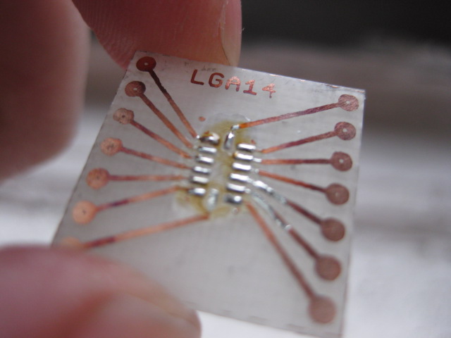
Sometimes you need to use a device and it's only available in surface mount form. In this article I describe an experiment that I conducted in order to create a DIP adapter for an LGA-14 SMT component (MMA7456L Accelerometer)
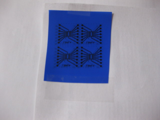
I started by creating the design of the breakout board PCB you can find the PDF here LGA14_BREAKOUT_BOARD.pdf.
Next I printed it on a piece of tonner transfer paper. To save transfer paper I first printed the design on a regular sheet of paper , then I cut a piece of transfer paper and taped it to the white sheet. Make sure you leave enough border – you don't want to print on the tape. After that the paper is fed again into the printer and the design is printed on the transfer paper this time.
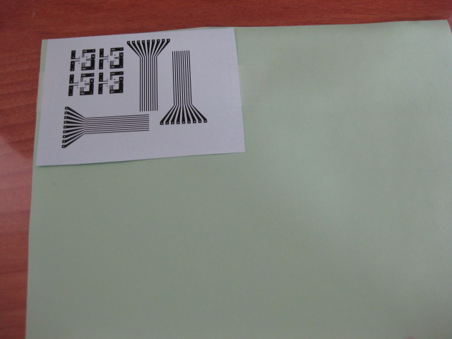
Similar thing with Pulsar Transfer Paper :
Next we need to transfer this onto a piece of copper clad board. Using an iron:
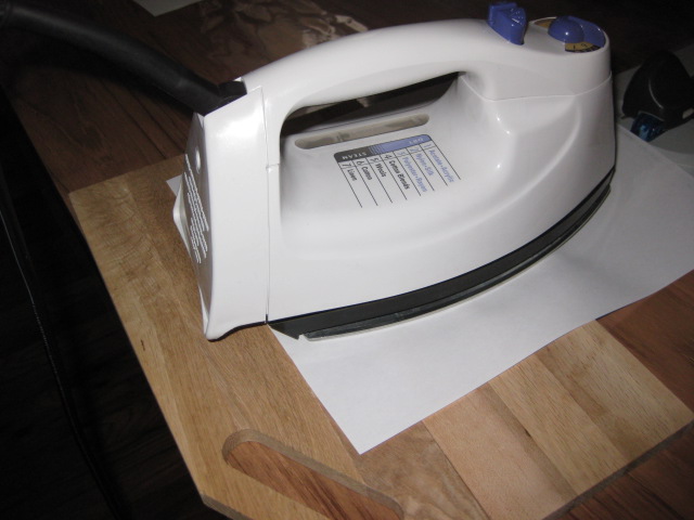
After 2-3 minutes of ironing the tonner will transfer to the board. Just run it under cold water and the transfer will peel off leaving the tonner on the copper board. If you fail first attempts chances are you did not cleaned your board (it must be shinny and uniform) or you did not apply enough heat. If your transfer comes out smudged or washed out it means you moved your iron too much in the first minutes. It is best to hold the iron still for the first 1-2 minutes and only the last minute actually move it a little to cover any uncovered spots. It's best to use an iron without holes (i.e. dry iron).
Another better way to transfer the toner to the PCB is to use a laminator, like this one that I picked up at an online store:
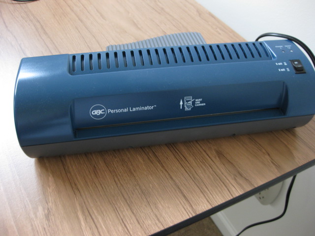
You'll find detailed instructions how to use the laminator at http://www.pulsarprofx.com/. They recommend using PCB not larger than 0.032", however regular width 0.064" should work with a little push.
You can use a sharpie to correct any broken traces, or scratch off any excess toner.
I got good results with the laminator with both Pulsar and Press-n-Peel transfer paper. The Pulsar paper however requires a second layer Green TRF to fill in any gaps in the toner transfer. Press-n-Peel on the other hand has poor adhesion , I passed the board 6 times through laminator and still got one place to correct with the sharpie (not major problem).
Next the board is placed in a PCB etching solution, please follow instructions on the bottle. Be careful wear gloves and eye protection.
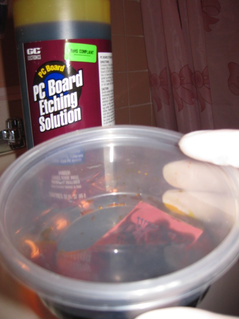
Use a plastic container with a secure lid to perform the etching. Place the container in warm water and shake it a little to accelerate the process. Choose a clear container so you can examine the board without removing it. Tilting the container will reveal part of the board – you'll see that the uncovered copper is "eaten" away. When all copper was etched – remove the board from etching solution and rinse it well under clean water. Use tweezers and gloves. Try to be neat – this stuff stains.
Another method is to place the board in a zip-lock bag (make it double for safety). Add the etchant to the bag and rub the board with your thingers (through the bag). Make sure you round-off any sharp edges of the board to avoid puncture. This method is reported to work fastest and uses minimum amount of etchant.
Just before you're ready to go ahead with the reflow remove the tonner (tonner will protect your coper from oxidation so leave it on if your board will be sitting unused for a while). To clean the tonner you can use acetone , or you can use ultra-fine sandpaper.
You should get something like this:
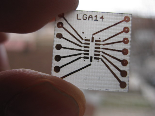
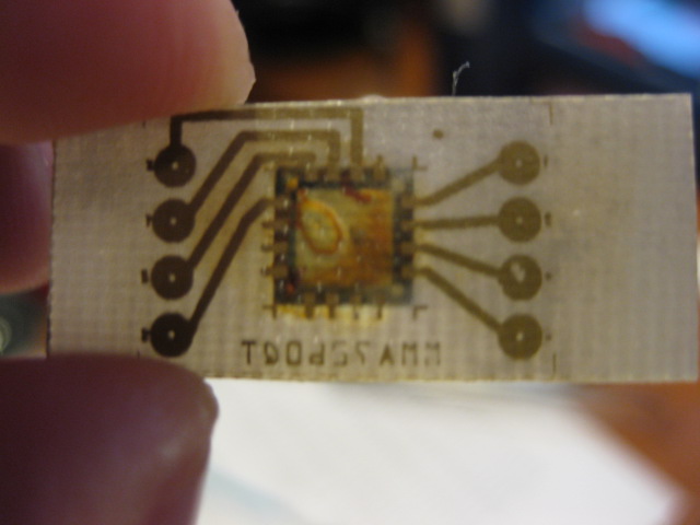
Notice that I chose a thin transparent PCB – this way I can inspect the traces under the device after the reflow process to make sure there are no shorts or unconnected pads.
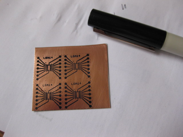
I created 4 boards on the same PCB so I just chose the one that came out better. Small imperfections will always happen with these DIY methods, just make sure there are no shorts or broken traces. The SMT pads should be even and well separated. However you can achieve near perfect results if you're using a laminator. I was able to get clear pads and traces of 10mil (0.25 mm) width.
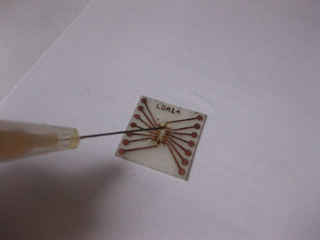
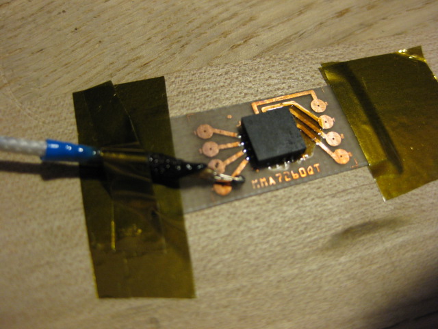
Next we'll apply solder to the SMT pads on the board and on the device pads. Before you do that apply flux to the pads:
Then with the tip of the iron holding a small amount of solder (more like a ball of solder), simply touch the pads with this ball. If you applied too much solder on a pad, wipe it off with a clean iron. The end result should look something like this:
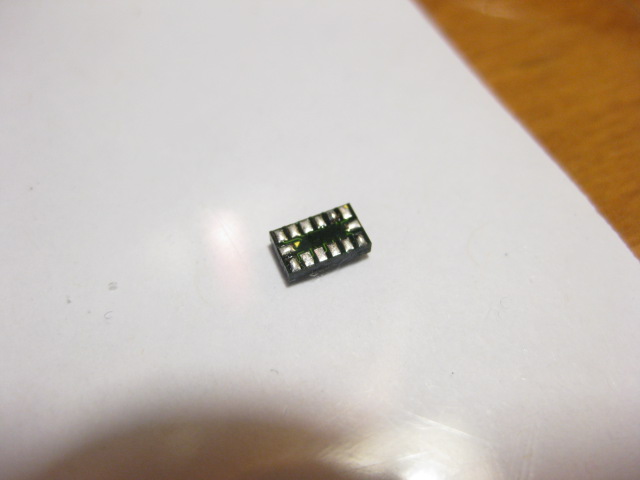
Do the same for the device:
And here is video walk-through:
We're ready now to start our reflow process. Place a little bit more flux on the pads, and place the board on a skillet. (I used a regular skillet and a gas stove ). Place the device on top of the PCB. Do your best effort to align PCB and device pads. It's ok if they are slightly misaligned since when solder reflows the two will snap in place.
Next, start heating the skillet. Slowly – or your flux will start to boil which will result in device being thrown away from it's place. If this happens , it's ok , place again a little flux and start the process again, this time be more patient and allow the pcb to heat up slower.
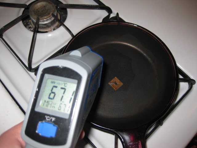
Monitor your temperature with a non-contact thermometer (or a contact thermometer) – when you reach 200-220C the solder will start to melt – you'll see that the device snaps in place. It's time to turn off your stove and carefully remove the skillet from stove.
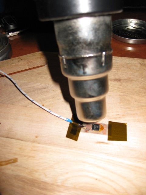
Another method to reflow is using a regular heat gun, put it at 590 deg F, and monitor the temperature using a multimiter at arround 500F the solder will reflow:
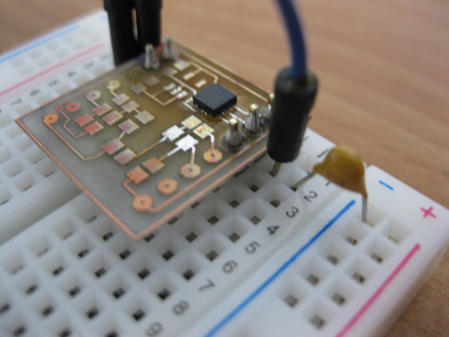
Let the board cool off and you're done, here is the final result after soldering some male headers:
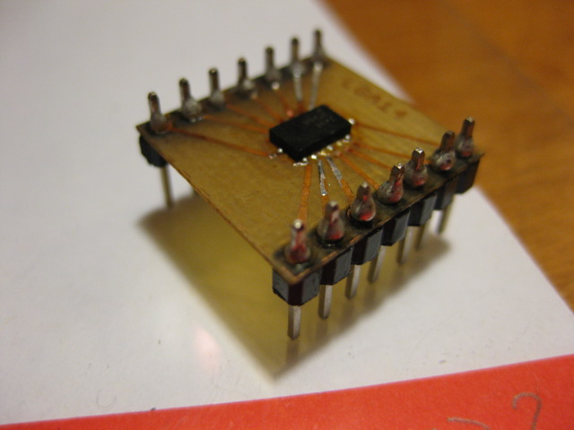
I can now mount this accelerometer on my breadboard or a DIP socket.
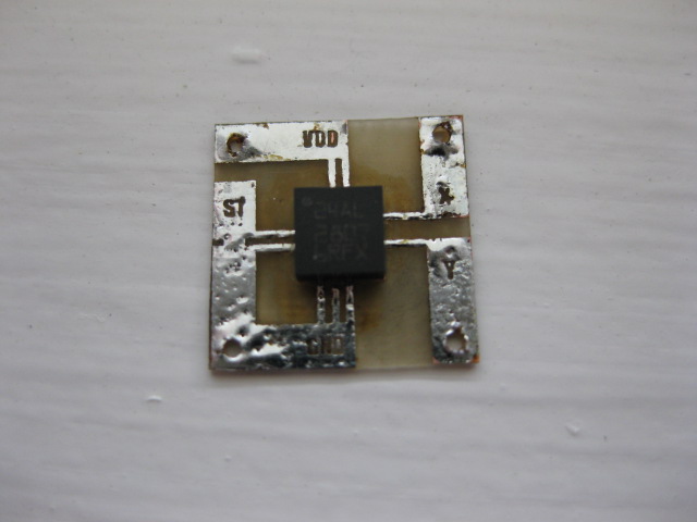
Finally here is the other example of finished product (LIS244AL accelerometer). Notice the surface is pourous since I dind't have Greet TRF at that time and my tonner was low. Here is the PDF for LIS244AL ACCELEROMETER – LGA16.
Here is another board, for a tiny LIS331AL accelerometer (3mm x 3mm).
//starlino//
Great idea! I was just wondering if you had a pdf for a LGA-16 chip as well?
Thanks,
Cory
I added the PDF for LIS244AL ACCELEROMETER (LGA16) right above the picture.
Hi there! Great post and great website!
I’m in starting to build my own breakout boards and I’m going to use a similar procedure to your.
The process I was going to use is actually the same until the coocking/reflow step.
I was thinking about using the soldering iron instead of the oven to reflow: basically after you have solder on the IC and the PCB you put your solder iron the the copper track and the heat let the solder to melt and connect the IC pins to the PCB.
I still did not try this process (need to wait for etchant – currently not available on my fav shop) but I was wondering: what do you think about? Do you think it would be possible?
Thanks,
Fabio Varesano
Fabio, you would need to heat all tracks at once … so you’ll need a very wide tip for your method to work. Nevertheless I admire your inventiveness.
Actually I was thinking about doing one pin a time. Of course it will be complex to align the ic on the PCB pads correctly.
I’m going to do this tomorrow. I’ll report here how it will work.
Finally I used the cooker method to solder and I can confirm that it works. See http://www.varesano.net/blog/fabio/homebrew-diy-breakout-board-adxl345-accelerometer-first-process-try-tested-arduino-proces for my result.
The above was the first test, now I’m getting more experienced.. I bought a low cost oven and solder paste and I’m now doing my designs with them. Cool stuff!
Hi, can you suggest an easy way to tile a footprint output from Eagle into a nice 2×2 panel as you have in your PDF? Thanks,
-Jordan
Jordan, you can use Avery Design Pro software (http://www.averyproducts.com.au/avery/en_au/Templates-&-Software/Software/Avery-DesignPro-5-Light-for-PC.htm) , basically it’s designed to print more than one label on a page, but you can use it for PCBs if you export it as an image from Eagle and then import it into this software.
Another method – you can open an exported file in adobe illustrator , create a symbol and then copy & paste it multiple times. Then once you update the symbol all other copies will update automatically. You can create such a template and then reuse it.
If you need to print to PDF from any software you can use CutePDF or other PDF printer.
this is a great post. I am trying to use the LIS2DH accelerometer which is LGA-14 2x2mm….
i am worried my traces at 8mils will be too thin, i’m about to find out!
what is the resolution of your printer?